- 您现在的位置:买卖IC网 > Sheet目录308 > ADUM3160BRWZ-RL (Analog Devices Inc)IC ISOLATOR USB 2.5K 16SOIC
�� ��
��
��Data� Sheet�
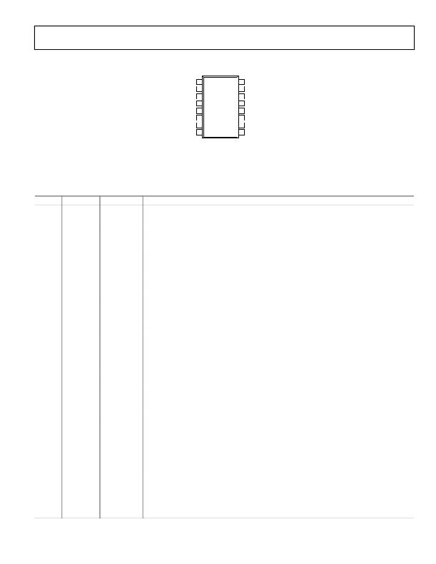
�PIN� CONFIGURATION� AND� FUNCTION� DESCRIPTIONS�
�ADuM3160�
�V� BUS1� 1�
�GND� 1� *� 2�
�16�
�15�
�V� BUS2�
�GND� 2� *�
�V� DD1� 3�
�PDEN� 4�
�SPU� 5�
�UD–� 6�
�UD+� 7�
�GND� 1� *� 8�
�ADuM3160�
�TOP� VIEW�
�(Not� to� Scale)�
�14�
�13�
�12�
�11�
�10�
�9�
�V� DD2�
�SPD�
�PIN�
�DD–�
�DD+�
�GND� 2� *�
�*PIN� 2� AND� PIN� 8� ARE� INTERNALLY� CONNECTED� TO� EACH� OTHER,� AND� IT�
�IS� RECOMMENDED� THAT� BOTH� PINS� BE� CONNECTED� TO� A� COMMON� GROUND.�
�PIN� 9� AND� PIN� 15� ARE� INTERNALLY� CONNECTED� TO� EACH� OTHER,� AND� IT�
�IS� RECOMMENDED� THAT� BOTH� PINS� BE� CONNECTED� TO� A� COMMON� GROUND.�
�Figure� 3.� Pin� Configuration�
�Table� 9.� Pin Function� Descriptions�
�Pin� No.�
�1�
�Mnemonic�
�V� BUS1�
�Direction�
�Power�
�Description�
�Input� Power� Supply� for� Side� 1.� When� the� isolator� is� powered� by� the� USB� bus� voltage� (4.5� V� to� 5.5� V),�
�connect� the� V� BUS1� pin� to� the� USB� power� bus.� When� the� isolator� is� powered� from� a� 3.3� V� power� supply,�
�connect� V� BUS1� to� V� DD1� and� to� the� external� 3.3� V� power� supply.� A� bypass� capacitor� to� GND� 1� is� required.�
�2�
�GND� 1�
�Return�
�Ground� 1.� Ground� reference� for� Isolator� Side� 1.� Pin� 2� and� Pin� 8� are� internally� connected� to� each�
�other,� and� it� is� recommended� that� both� pins� be� connected� to� a� common� ground.�
�3�
�V� DD1�
�Power�
�Input� Power� Supply� for� Side� 1.� When� the� isolator� is� powered� by� the� USB� bus� voltage� (4.5� V� to� 5.5� V),�
�the� V� DD1� pin� should� be� used� for� a� bypass� capacitor� to� GND� 1� .� Signal� lines� that� may� require� pull-up,� such�
�as� PDEN� and� SPU,� should� be� tied� to� this� pin.� When� the� isolator� is� powered� from� a� 3.3� V� power� supply,�
�connect� V� BUS1� to� V� DD1� and� to� the� external� 3.3� V� power� supply.� A� bypass� capacitor� to� GND� 1� is� required.�
�4�
�PDEN�
�Input�
�Pull-Down� Enable.� This� pin� is� read� when� exiting� reset.� This� pin� must� be� connected� to� V� DD1� for� standard�
�operation.� If� this� pin� is� connected� to� GND� 1� when� exiting� reset,� the� downstream� pull-down� resistors�
�are� disconnected,� allowing� buffer� impedance� measurements.�
�5�
�SPU�
�Input�
�Speed� Select,� Upstream� Buffer.� Active� high� logic� input.� When� SPU� is� tied� high,� the� full� speed� slew�
�rate,� timing,� and� logic� conventions� are� selected;� when� SPU� is� tied� low,� the� low� speed� slew� rate,�
�timing,� and� logic� conventions� are� selected.� This� input� must� be� set� high� via� connection� to� V� DD1� or� set�
�low� via� connection� to� GND� 1� and� must� match� Pin� 13� (both� pins� tied� high� or� both� pins� tied� low).�
�6�
�7�
�8�
�9�
�10�
�11�
�12�
�UD?�
�UD+�
�GND� 1�
�GND� 2�
�DD+�
�DD?�
�PIN�
�Input/Output�
�Input/Output�
�Return�
�Return�
�Input/Output�
�Input/Output�
�Input�
�Upstream� D?.�
�Upstream� D+.�
�Ground� 1.� Ground� reference� for� Isolator� Side� 1.� Pin� 2� and� Pin� 8� are� internally� connected� to� each�
�other,� and� it� is� recommended� that� both� pins� be� connected� to� a� common� ground.�
�Ground� 2.� Ground� reference� for� Isolator� Side� 2.� Pin� 9� and� Pin� 15� are� internally� connected� to� each�
�other,� and� it� is� recommended� that� both� pins� be� connected� to� a� common� ground.�
�Downstream� D+.�
�Downstream� D?.�
�Upstream� Pull-Up� Enable.� PIN� controls� the� power� connection� to� the� pull-up� for� the� upstream� port.�
�It� can� be� tied� to� V� DD2� for� operation� on� power-up,� or� it� can� be� tied� to� an� external� control� signal� for� an�
�application� that� requires� delayed� enumeration.�
�13�
�SPD�
�Input�
�Speed� Select,� Downstream� Buffer.� Active� high� logic� input.� When� SPD� is� tied� high,� the� full� speed�
�slew� rate,� timing,� and� logic� conventions� are� selected;� when� SPD� is� tied� low,� the� low� speed� slew� rate,�
�timing,� and� logic� conventions� are� selected.� This� input� must� be� set� high� via� connection� to� V� DD2� or� set�
�low� via� connection� to� GND� 2� and� must� match� Pin� 5� (both� pins� tied� high� or� both� pins� tied� low).�
�14�
�V� DD2�
�Power�
�Input� Power� Supply� for� Side� 2.� When� the� isolator� is� powered� by� the� USB� bus� voltage� (4.5� V� to� 5.5� V),�
�the� V� DD2� pin� should� be� used� for� a� bypass� capacitor� to� GND� 2� .� Signal� lines� that� may� require� pull-up,�
�such� as� SPD,� can� be� tied� to� this� pin.� When� the� isolator� is� powered� from� a� 3.3� V� power� supply,� connect�
�V� BUS2� to� V� DD2� and� to� the� external� 3.3� V� power� supply.� A� bypass� capacitor� to� GND� 2� is� required.�
�15�
�GND� 2�
�Return�
�Ground� 2.� Ground� reference� for� Isolator� Side� 2.� Pin� 9� and� Pin� 15� are� internally� connected� to� each�
�other,� and� it� is� recommended� that� both� pins� be� connected� to� a� common� ground.�
�16�
�V� BUS2�
�Power�
�Input� Power� Supply� for� Side� 2.� When� the� isolator� is� powered� by� the� USB� bus� voltage� (4.5� V� to� 5.5� V),�
�connect� the� V� BUS2� pin� to� the� USB� power� bus.� When� the� isolator� is� powered� from� a� 3.3� V� power� supply,�
�connect V� BUS2� to V� DD2� and to the external 3.3 V power supply. A bypass capacitor to GND� 2� is required.�
�Rev.� C� |� Page� 7� of� 16�
�发布紧急采购,3分钟左右您将得到回复。
相关PDF资料
ADUM3201WCRZ
ISOLATOR DGTL 25MBPS 2CH 8SOIC
ADUM3210WCRZ
IC DIGITAL ISOLATOR 2CH 8-SOIC
ADUM3300CRWZ
IC DIGITAL ISOLATOR 3CH 16-SOIC
ADUM3400BRWZ
IC DIGITAL ISOLATOR 4CH 16-SOIC
ADUM3442CRWZ-RL
IC DIGITAL ISOLATOR 4CHAN 16SOIC
ADUM4223BRWZ
ISOLATOR DIGITAL
ADUM4402CRWZ
IC DIGITAL ISOLATOR 4CH 16-SOIC
ADUM5000ARWZ-RL
IC DIG ISOLATOR W/DC-DC 16SOIC
相关代理商/技术参数
ADUM3160WBRWZ
功能描述:USB Digital Isolator 2500Vrms 2 Channel 12Mbps 25kV/μs CMTI 16-SOIC (0.295", 7.50mm Width) 制造商:analog devices inc. 系列:iCoupler? 包装:管件 零件状态:有效 技术:磁耦合 类型:USB 隔离式电源:无 通道数:2 输入 - 输入侧 1/输入侧 2:2/2 通道类型:双向 电压 - 隔离:2500Vrms 共模瞬态抗扰度(最小值):25kV/μs 数据速率:12Mbps 传播延迟 tpLH / tpHL(最大值):70ns,70ns 脉宽失真(最大):- 上升/下降时间(典型值):20ns,20ns(最大) 电压 - 电源:3 V ~ 5.5 V 工作温度:-40°C ~ 105°C 封装/外壳:16-SOIC(0.295",7.50mm 宽) 供应商器件封装:16-SOIC 标准包装:47
ADUM3160WBRWZ-RL
功能描述:USB Digital Isolator 2500Vrms 2 Channel 12Mbps 25kV/μs CMTI 16-SOIC (0.295", 7.50mm Width) 制造商:analog devices inc. 系列:iCoupler? 包装:带卷(TR) 零件状态:有效 技术:磁耦合 类型:USB 隔离式电源:无 通道数:2 输入 - 输入侧 1/输入侧 2:2/2 通道类型:双向 电压 - 隔离:2500Vrms 共模瞬态抗扰度(最小值):25kV/μs 数据速率:12Mbps 传播延迟 tpLH / tpHL(最大值):70ns,70ns 脉宽失真(最大):- 上升/下降时间(典型值):20ns,20ns(最大) 电压 - 电源:3 V ~ 5.5 V 工作温度:-40°C ~ 105°C 封装/外壳:16-SOIC(0.295",7.50mm 宽) 供应商器件封装:16-SOIC 标准包装:1,000
ADUM3190
制造商:AD 制造商全称:Analog Devices 功能描述:High Stability Isolated Error Amplifier
ADUM3190_13
制造商:AD 制造商全称:Analog Devices 功能描述:High Stability Isolated Error Amplifier
ADUM3190ARQZ
功能描述:隔离放大器
RoHS:否 制造商:Texas Instruments 输入补偿电压:1.5 mV 共模抑制比(最小值):95 dB 带宽:60 KHz 工作电源电压:3.3 V 电源电流:8 mA 工作温度范围:- 40 C to + 105 C 安装风格:SMD/SMT 封装 / 箱体:SOP-8 封装:Tube
ADUM3190ARQZ-RL7
功能描述:隔离放大器
RoHS:否 制造商:Texas Instruments 输入补偿电压:1.5 mV 共模抑制比(最小值):95 dB 带宽:60 KHz 工作电源电压:3.3 V 电源电流:8 mA 工作温度范围:- 40 C to + 105 C 安装风格:SMD/SMT 封装 / 箱体:SOP-8 封装:Tube
ADUM3190BRQZ
功能描述:隔离放大器
RoHS:否 制造商:Texas Instruments 输入补偿电压:1.5 mV 共模抑制比(最小值):95 dB 带宽:60 KHz 工作电源电压:3.3 V 电源电流:8 mA 工作温度范围:- 40 C to + 105 C 安装风格:SMD/SMT 封装 / 箱体:SOP-8 封装:Tube
ADUM3190BRQZ-RL7
功能描述:隔离放大器
RoHS:否 制造商:Texas Instruments 输入补偿电压:1.5 mV 共模抑制比(最小值):95 dB 带宽:60 KHz 工作电源电压:3.3 V 电源电流:8 mA 工作温度范围:- 40 C to + 105 C 安装风格:SMD/SMT 封装 / 箱体:SOP-8 封装:Tube