- 您现在的位置:买卖IC网 > Sheet目录308 > ADUM3160BRWZ-RL (Analog Devices Inc)IC ISOLATOR USB 2.5K 16SOIC
Data Sheet
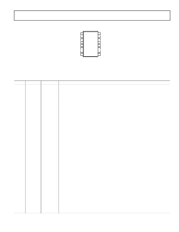
PIN CONFIGURATION AND FUNCTION DESCRIPTIONS
ADuM3160
V BUS1 1
GND 1 * 2
16
15
V BUS2
GND 2 *
V DD1 3
PDEN 4
SPU 5
UD– 6
UD+ 7
GND 1 * 8
ADuM3160
TOP VIEW
(Not to Scale)
14
13
12
11
10
9
V DD2
SPD
PIN
DD–
DD+
GND 2 *
*PIN 2 AND PIN 8 ARE INTERNALLY CONNECTED TO EACH OTHER, AND IT
IS RECOMMENDED THAT BOTH PINS BE CONNECTED TO A COMMON GROUND.
PIN 9 AND PIN 15 ARE INTERNALLY CONNECTED TO EACH OTHER, AND IT
IS RECOMMENDED THAT BOTH PINS BE CONNECTED TO A COMMON GROUND.
Figure 3. Pin Configuration
Table 9. Pin Function Descriptions
Pin No.
1
Mnemonic
V BUS1
Direction
Power
Description
Input Power Supply for Side 1. When the isolator is powered by the USB bus voltage (4.5 V to 5.5 V),
connect the V BUS1 pin to the USB power bus. When the isolator is powered from a 3.3 V power supply,
connect V BUS1 to V DD1 and to the external 3.3 V power supply. A bypass capacitor to GND 1 is required.
2
GND 1
Return
Ground 1. Ground reference for Isolator Side 1. Pin 2 and Pin 8 are internally connected to each
other, and it is recommended that both pins be connected to a common ground.
3
V DD1
Power
Input Power Supply for Side 1. When the isolator is powered by the USB bus voltage (4.5 V to 5.5 V),
the V DD1 pin should be used for a bypass capacitor to GND 1 . Signal lines that may require pull-up, such
as PDEN and SPU, should be tied to this pin. When the isolator is powered from a 3.3 V power supply,
connect V BUS1 to V DD1 and to the external 3.3 V power supply. A bypass capacitor to GND 1 is required.
4
PDEN
Input
Pull-Down Enable. This pin is read when exiting reset. This pin must be connected to V DD1 for standard
operation. If this pin is connected to GND 1 when exiting reset, the downstream pull-down resistors
are disconnected, allowing buffer impedance measurements.
5
SPU
Input
Speed Select, Upstream Buffer. Active high logic input. When SPU is tied high, the full speed slew
rate, timing, and logic conventions are selected; when SPU is tied low, the low speed slew rate,
timing, and logic conventions are selected. This input must be set high via connection to V DD1 or set
low via connection to GND 1 and must match Pin 13 (both pins tied high or both pins tied low).
6
7
8
9
10
11
12
UD?
UD+
GND 1
GND 2
DD+
DD?
PIN
Input/Output
Input/Output
Return
Return
Input/Output
Input/Output
Input
Upstream D?.
Upstream D+.
Ground 1. Ground reference for Isolator Side 1. Pin 2 and Pin 8 are internally connected to each
other, and it is recommended that both pins be connected to a common ground.
Ground 2. Ground reference for Isolator Side 2. Pin 9 and Pin 15 are internally connected to each
other, and it is recommended that both pins be connected to a common ground.
Downstream D+.
Downstream D?.
Upstream Pull-Up Enable. PIN controls the power connection to the pull-up for the upstream port.
It can be tied to V DD2 for operation on power-up, or it can be tied to an external control signal for an
application that requires delayed enumeration.
13
SPD
Input
Speed Select, Downstream Buffer. Active high logic input. When SPD is tied high, the full speed
slew rate, timing, and logic conventions are selected; when SPD is tied low, the low speed slew rate,
timing, and logic conventions are selected. This input must be set high via connection to V DD2 or set
low via connection to GND 2 and must match Pin 5 (both pins tied high or both pins tied low).
14
V DD2
Power
Input Power Supply for Side 2. When the isolator is powered by the USB bus voltage (4.5 V to 5.5 V),
the V DD2 pin should be used for a bypass capacitor to GND 2 . Signal lines that may require pull-up,
such as SPD, can be tied to this pin. When the isolator is powered from a 3.3 V power supply, connect
V BUS2 to V DD2 and to the external 3.3 V power supply. A bypass capacitor to GND 2 is required.
15
GND 2
Return
Ground 2. Ground reference for Isolator Side 2. Pin 9 and Pin 15 are internally connected to each
other, and it is recommended that both pins be connected to a common ground.
16
V BUS2
Power
Input Power Supply for Side 2. When the isolator is powered by the USB bus voltage (4.5 V to 5.5 V),
connect the V BUS2 pin to the USB power bus. When the isolator is powered from a 3.3 V power supply,
connect V BUS2 to V DD2 and to the external 3.3 V power supply. A bypass capacitor to GND 2 is required.
Rev. C | Page 7 of 16
发布紧急采购,3分钟左右您将得到回复。
相关PDF资料
ADUM3201WCRZ
ISOLATOR DGTL 25MBPS 2CH 8SOIC
ADUM3210WCRZ
IC DIGITAL ISOLATOR 2CH 8-SOIC
ADUM3300CRWZ
IC DIGITAL ISOLATOR 3CH 16-SOIC
ADUM3400BRWZ
IC DIGITAL ISOLATOR 4CH 16-SOIC
ADUM3442CRWZ-RL
IC DIGITAL ISOLATOR 4CHAN 16SOIC
ADUM4223BRWZ
ISOLATOR DIGITAL
ADUM4402CRWZ
IC DIGITAL ISOLATOR 4CH 16-SOIC
ADUM5000ARWZ-RL
IC DIG ISOLATOR W/DC-DC 16SOIC
相关代理商/技术参数
ADUM3160WBRWZ
功能描述:USB Digital Isolator 2500Vrms 2 Channel 12Mbps 25kV/μs CMTI 16-SOIC (0.295", 7.50mm Width) 制造商:analog devices inc. 系列:iCoupler? 包装:管件 零件状态:有效 技术:磁耦合 类型:USB 隔离式电源:无 通道数:2 输入 - 输入侧 1/输入侧 2:2/2 通道类型:双向 电压 - 隔离:2500Vrms 共模瞬态抗扰度(最小值):25kV/μs 数据速率:12Mbps 传播延迟 tpLH / tpHL(最大值):70ns,70ns 脉宽失真(最大):- 上升/下降时间(典型值):20ns,20ns(最大) 电压 - 电源:3 V ~ 5.5 V 工作温度:-40°C ~ 105°C 封装/外壳:16-SOIC(0.295",7.50mm 宽) 供应商器件封装:16-SOIC 标准包装:47
ADUM3160WBRWZ-RL
功能描述:USB Digital Isolator 2500Vrms 2 Channel 12Mbps 25kV/μs CMTI 16-SOIC (0.295", 7.50mm Width) 制造商:analog devices inc. 系列:iCoupler? 包装:带卷(TR) 零件状态:有效 技术:磁耦合 类型:USB 隔离式电源:无 通道数:2 输入 - 输入侧 1/输入侧 2:2/2 通道类型:双向 电压 - 隔离:2500Vrms 共模瞬态抗扰度(最小值):25kV/μs 数据速率:12Mbps 传播延迟 tpLH / tpHL(最大值):70ns,70ns 脉宽失真(最大):- 上升/下降时间(典型值):20ns,20ns(最大) 电压 - 电源:3 V ~ 5.5 V 工作温度:-40°C ~ 105°C 封装/外壳:16-SOIC(0.295",7.50mm 宽) 供应商器件封装:16-SOIC 标准包装:1,000
ADUM3190
制造商:AD 制造商全称:Analog Devices 功能描述:High Stability Isolated Error Amplifier
ADUM3190_13
制造商:AD 制造商全称:Analog Devices 功能描述:High Stability Isolated Error Amplifier
ADUM3190ARQZ
功能描述:隔离放大器
RoHS:否 制造商:Texas Instruments 输入补偿电压:1.5 mV 共模抑制比(最小值):95 dB 带宽:60 KHz 工作电源电压:3.3 V 电源电流:8 mA 工作温度范围:- 40 C to + 105 C 安装风格:SMD/SMT 封装 / 箱体:SOP-8 封装:Tube
ADUM3190ARQZ-RL7
功能描述:隔离放大器
RoHS:否 制造商:Texas Instruments 输入补偿电压:1.5 mV 共模抑制比(最小值):95 dB 带宽:60 KHz 工作电源电压:3.3 V 电源电流:8 mA 工作温度范围:- 40 C to + 105 C 安装风格:SMD/SMT 封装 / 箱体:SOP-8 封装:Tube
ADUM3190BRQZ
功能描述:隔离放大器
RoHS:否 制造商:Texas Instruments 输入补偿电压:1.5 mV 共模抑制比(最小值):95 dB 带宽:60 KHz 工作电源电压:3.3 V 电源电流:8 mA 工作温度范围:- 40 C to + 105 C 安装风格:SMD/SMT 封装 / 箱体:SOP-8 封装:Tube
ADUM3190BRQZ-RL7
功能描述:隔离放大器
RoHS:否 制造商:Texas Instruments 输入补偿电压:1.5 mV 共模抑制比(最小值):95 dB 带宽:60 KHz 工作电源电压:3.3 V 电源电流:8 mA 工作温度范围:- 40 C to + 105 C 安装风格:SMD/SMT 封装 / 箱体:SOP-8 封装:Tube
